

Differences between Scanning Electron Microscopy and Transmission Electron Microscopy
| Properties | Scanning Electron Microscopy | Transmission Electron Microscopy |
| Light Source | SEM is based on scattered electrons, i.e. electrons emitted from the surface of a specimen. It is the EM analog of a stereo light microscope. | TEM is based on transmitted electrons and operates on the same basic principles as the light microscope. |
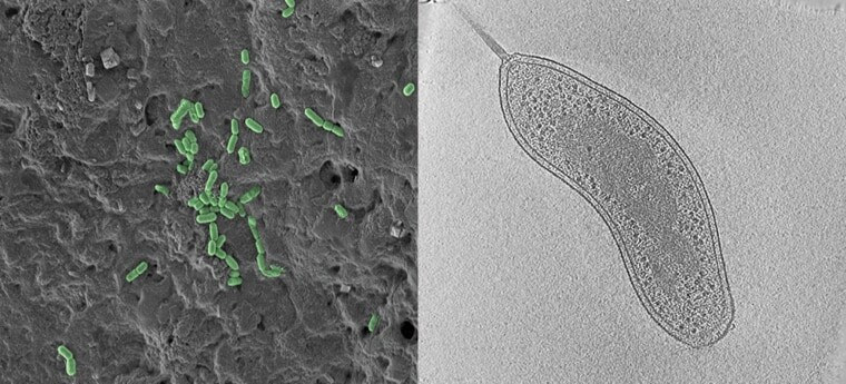
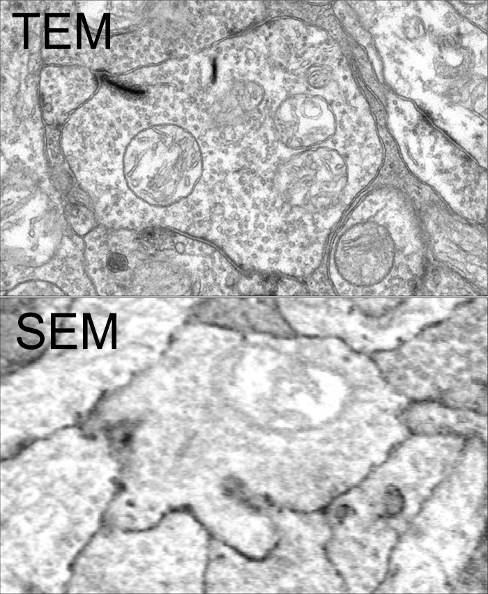
| Purpose | SEM provides detailed images of the surfaces of cells. SEM focuses on the sample’s surface and its composition, so SEM shows only the morphology of samples. | TEM is used to view thin specimens. TEM can show many characteristics of the sample, such as internal composition, morphology, crystallization, etc |
| Sample Preparation | Sample is coated with a thin layer of heavy metal such as gold or palladium. | The sample in TEM has to be cut thinner (70-90 nm) because electrons cannot penetrate very far into materials. |
| Processing of sample (s) | SEM allows for a large amount of sample to be analyzed at a time. | With TEM only a small amount of samples can be analyzed at a time. |
| Resolution | SEM can resolve objects as close as 20 nm. | TEM has a much higher resolution than SEM. It can resolve objects as close as 1 nm i.e. down to near-atomic levels. |
| Magnification | The magnifying power of SEM is up to 50000X | The magnifying power of TEM is up to 2 million times. |
| Image formation | Secondary or backscattered electrons arising from the interaction of electron beam and metal coated specimen are collected and the resulting image is displayed on a computer screen. | Transmitted electrons hit a fluorescent screen giving rise to a “shadow image” of the specimen with its different parts displayed in varied darkness according to their density. The image can be studied directly by the operator or photographed with a camera. |
| 3D picture | To study topography and atomic composition of specimens, process control and also, for example, the surface distribution of immunolabels. | To image the interior of cells, the structure of protein molecules, the organization of molecules in viruses and cytoskeletal filaments, and the arrangement of protein molecules in cell membranes. |
Working principle of Transmission Electron Microscopy (TEM)
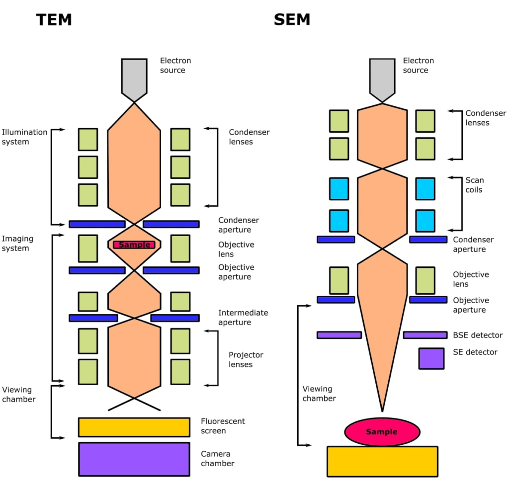
The working principle of Transmission Electron Microscopy (TEM) is based on the interaction of a high-energy electron beam with a thin specimen as the beam passes through it. The fundamental components of a TEM include an electron source, electromagnetic lenses, a vacuum system, and imaging devices. The detailed working principle can be described as follows:
Electron Source and Acceleration
- In a TEM, electrons are typically generated from a thermionic or field emission source.
- A thermionic source, such as a tungsten or lanthanum hexaboride (LaB6) filament, emits electrons when heated to high temperatures (typically around 2700 K).
- Field emission sources, such as tungsten hairpin or single-crystal tungsten tips, emit electrons under the influence of a strong electric field (typically around 10^9 V/m).
- The emitted electrons are accelerated by a high voltage (typically ranging from 60 kV to 300 kV) to achieve high kinetic energies, which are necessary for adequate penetration through the specimen.
Electron Beam Formation and Manipulation
- A series of electromagnetic lenses, including condenser lenses, are employed to focus and manipulate the electron beam before it interacts with the specimen.
- The condenser lenses control the beam size, intensity, and convergence angle, allowing for precise adjustment of the beam characteristics.
- Apertures are used to select specific portions of the electron beam, enabling various imaging and diffraction techniques.
Specimen Interaction
- The specimen must be sufficiently thin (typically less than 100 nm) to allow the electron beam to pass through it.
- As the high-energy electrons interact with the specimen, they can undergo elastic or inelastic scattering, depending on the specimen’s atomic structure, density, and thickness.
- Elastic scattering, which involves a change in the electron’s direction but not its energy, provides information about the specimen’s structure and crystallinity.
- Inelastic scattering, which involves energy loss, provides information about the specimen’s chemical composition and electronic structure.
Image Formation
- The transmitted electrons, which have interacted with the specimen, are focused by the objective lens onto an imaging device, such as a fluorescent screen or a charge-coupled device (CCD) camera.
- The image is formed based on the varying intensities of the transmitted electrons, which depend on the specimen’s properties and the specific contrast mechanism employed.
Contrast Mechanisms
- TEM images can exhibit different contrast mechanisms, including mass-thickness contrast, diffraction contrast, and phase contrast, providing information about the specimen’s structure, crystallinity, and defects.
- Mass-thickness contrast arises from the difference in the scattering of electrons by regions with varying mass and thickness within the specimen.
- Diffraction contrast is generated by the interaction of electrons with the crystalline structure of the specimen, revealing information about crystal defects, grain boundaries, and orientations.
- Phase contrast is achieved by introducing phase shifts in the electron wave function, enabling the visualization of subtle features that would otherwise be invisible.
Imaging Modes
- TEM offers various imaging modes, such as bright-field (BF) imaging, dark-field (DF) imaging, and high-resolution TEM (HRTEM) for atomic-scale imaging.
- Bright-field imaging is the most common mode, where the directly transmitted electrons form the image.
- Dark-field imaging utilizes scattered or diffracted electrons, revealing specific crystallographic orientations or defects.
- HRTEM employs phase contrast techniques to achieve sub-angstrom resolution, allowing for direct visualization of atomic structures and defects.
Analytical Techniques
- TEM can be coupled with various analytical techniques, such as energy-dispersive X-ray spectroscopy (EDS) and electron energy loss spectroscopy (EELS), for chemical analysis and elemental mapping.
- EDS detects characteristic X-rays emitted by the specimen when excited by the electron beam, providing information about the elemental composition.
- EELS measures the energy loss of electrons after interacting with the specimen, revealing information about electronic structures and chemical bonding.
TEM’s exceptional resolution, down to sub-angstrom levels, and its ability to provide structural, crystallographic, and compositional information make it an invaluable tool for studying materials at the atomic and nanoscale, such as nanoparticles, thin films, and biological specimens like viruses and proteins.
The working principle of Scanning Electron Microscopy (SEM)
The working principle of Scanning Electron Microscopy (SEM) is based on scanning a focused electron beam across the surface of a specimen and detecting the various signals generated by the interaction between the electron beam and the specimen. The key components of an SEM include an electron source, electromagnetic lenses, scanning coils, detectors, and a vacuum system. The detailed working principle can be described as follows:
Electron Source and Acceleration
- Similar to TEM, an electron gun (thermionic or field emission) generates and accelerates electrons, typically in the range of 1-30 keV.
- Thermionic sources, such as tungsten or lanthanum hexaboride (LaB6) filaments, emit electrons when heated to high temperatures.
- Field emission sources, like tungsten hairpin or single-crystal tungsten tips, emit electrons under the influence of a strong electric field.
Electron Beam Formation and Scanning
- Electromagnetic lenses focus the electron beam into a fine probe, which is then scanned over the specimen’s surface in a raster pattern by scanning coils.
- The scanning coils precisely control the position of the electron beam, allowing it to systematically scan across the specimen’s surface.
Specimen Interaction
- As the focused electron beam interacts with the specimen’s surface, various signals are generated, including secondary electrons, backscattered electrons, and characteristic X-rays.
- Secondary electrons are low-energy electrons emitted from the specimen’s surface due to inelastic scattering of the primary beam electrons. These electrons provide information about the specimen’s surface topography.
- Backscattered electrons are high-energy electrons that have undergone elastic scattering by the specimen’s atomic nuclei. These electrons provide information about the specimen’s composition and crystallographic orientation.
- Characteristic X-rays are emitted when the primary beam electrons ionize the specimen’s atoms, and electrons from higher energy levels fill the vacancies, releasing X-rays with energies characteristic of the element.
Signal Detection
- Specialized detectors collect the emitted signals, which are then amplified and processed to form an image.
- Secondary electron detectors, such as Everhart-Thornley detectors or in-lens detectors, collect and amplify secondary electrons, providing high-resolution topographic information.
- Backscattered electron detectors, such as solid-state or scintillator detectors, collect and amplify backscattered electrons, providing compositional and crystallographic information.
- Energy-dispersive X-ray spectroscopy (EDS) detectors analyze the characteristic X-rays emitted from the specimen, enabling elemental composition analysis
Image Formation
- The detected signals are used to modulate the brightness of a cathode ray tube (CRT) or a digital image, creating a high-resolution image of the specimen’s surface.
- The brightness of each pixel in the image is proportional to the intensity of the detected signal at the corresponding point on the specimen’s surface.
Imaging Modes
- SEM offers various imaging modes, such as secondary electron (SE) imaging for topography, backscattered electron (BSE) imaging for compositional contrast, and analytical techniques like EDS for elemental analysis.
- SE imaging is the most common mode, providing detailed information about the specimen’s surface features and topography.
- BSE imaging reveals compositional variations within the specimen, as heavier elements appear brighter due to their higher backscattering efficiency.
- EDS analysis allows for the identification and quantification of the elements present in the specimen, enabling elemental mapping and analysis.
Sample Preparation
- SEM requires specimens to be electrically conductive to prevent charging effects and enable efficient signal detection.
- Non-conductive specimens are typically coated with a thin layer of conductive material, such as gold, carbon, or a combination of metals, using techniques like sputter coating or evaporation.
- Sample preparation techniques, such as fracturing, polishing, or etching, may be employed to reveal specific features or structures of interest.
SEM’s ability to provide high-resolution images of surface topography, combined with analytical capabilities like EDS, makes it invaluable for studying the morphology, composition, and microstructure of materials in fields such as materials science, geology, biology, and semiconductor industries. Its versatility and ease of sample preparation make it a widely used technique in various research and industrial applications.